
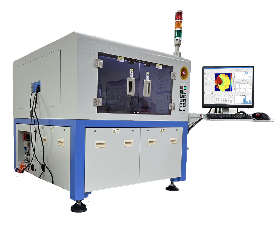
Non-destructive Wafer and Material Analysis
The quality of the material determines the maximum achievable conversion efficiency to the final device. Conventional optical inspection systems rely on VIS/ IR optical detectors that can only check the surface phenomenon of the device under test (DUT) but can not measure the internal structures and the physical properties of the DUT.
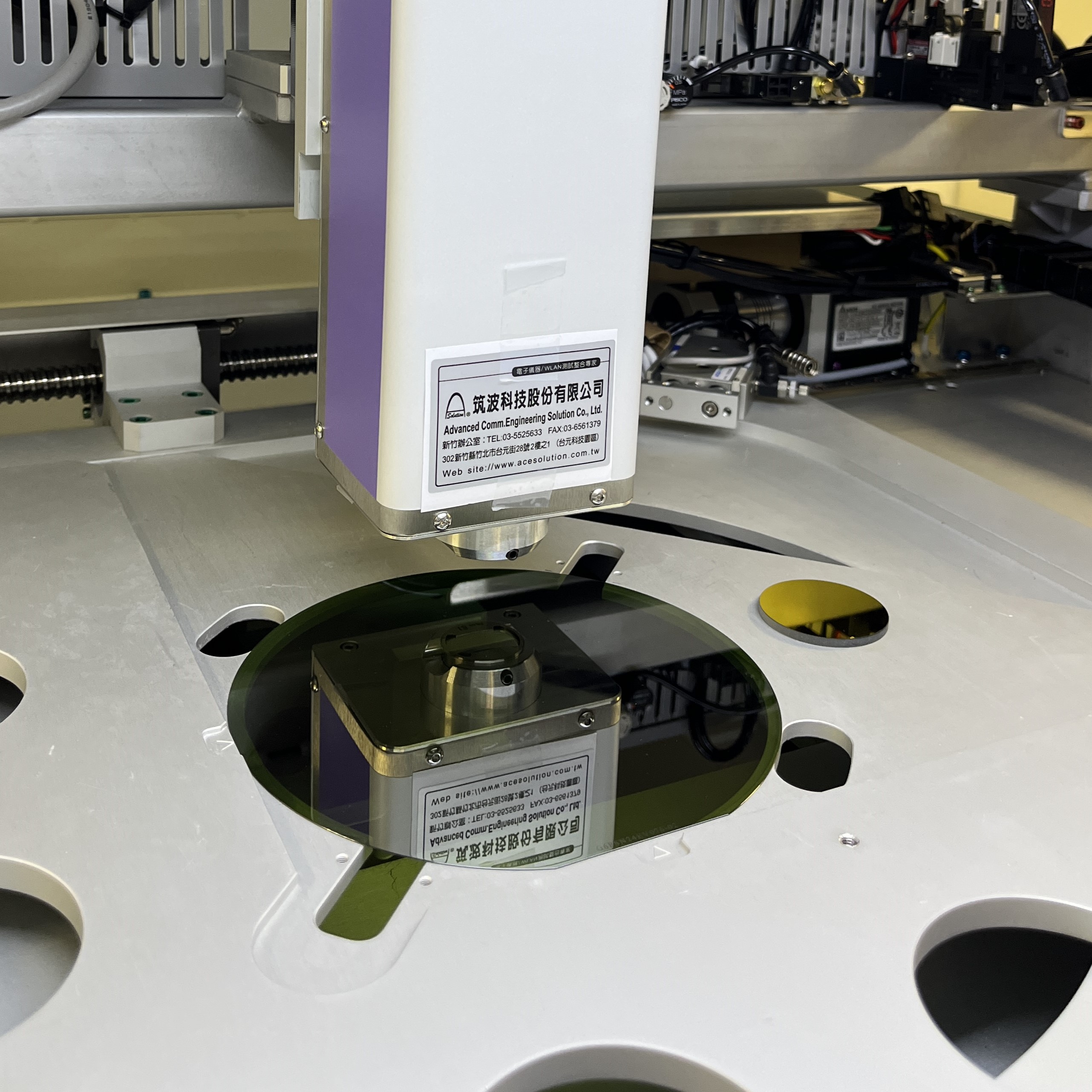
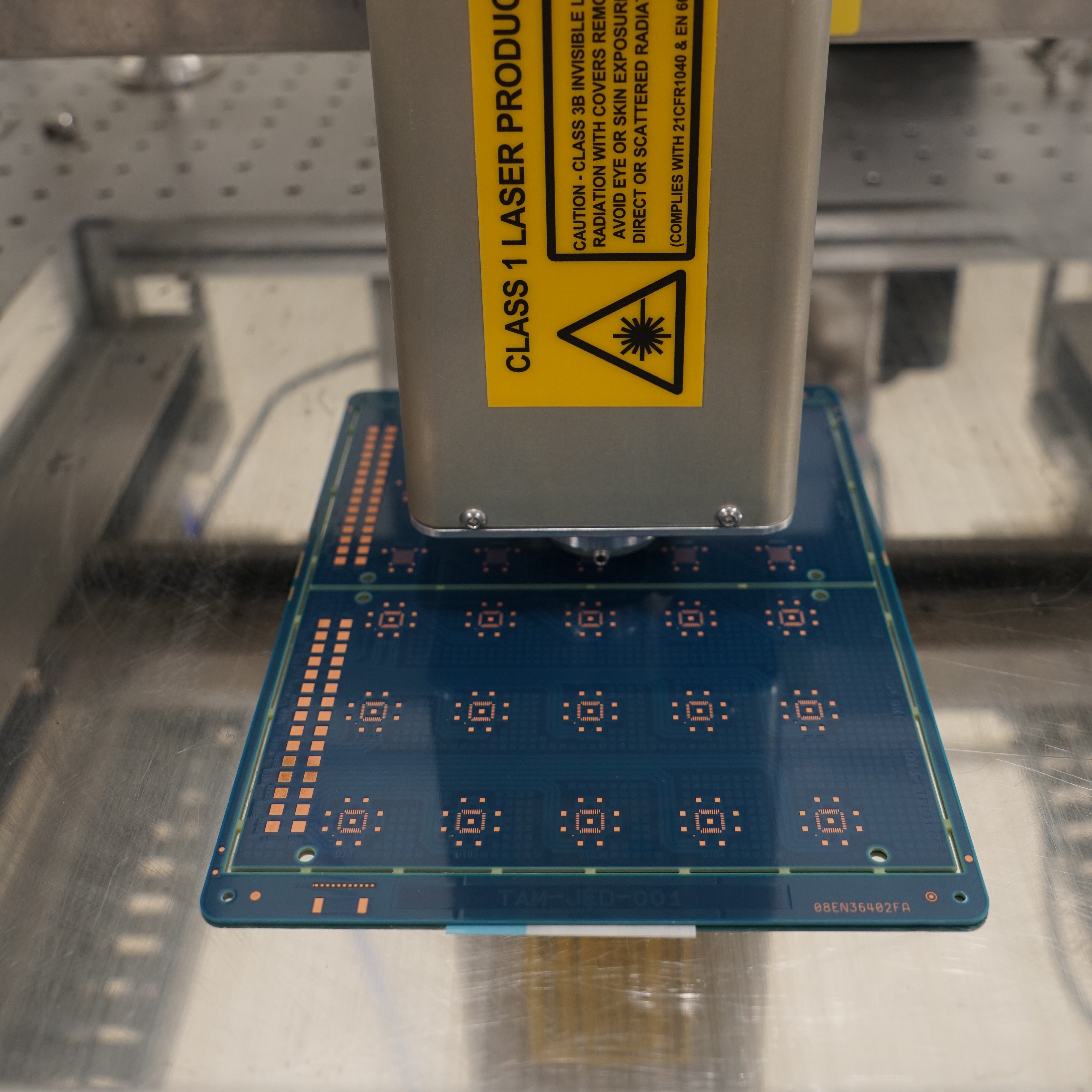
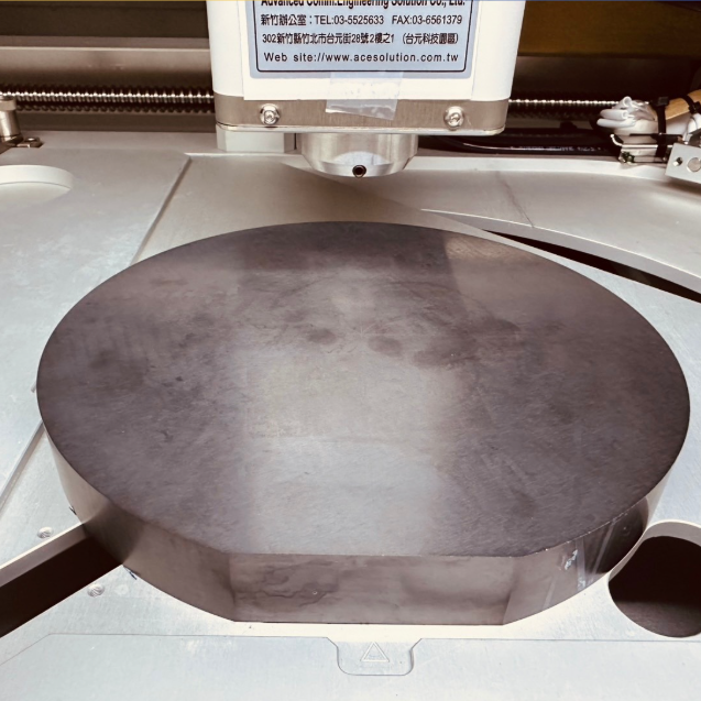
Terahertz (THz) waves can penetrate various low-dielectric materials, including wood, plastics, ceramics, and semiconductor wafers, and enable direct measurement of samples' complex refractive index and absorption coefficient by analyzing the sample-induced changes in a transmitted or reflected THz signals.
 |
 |
|
Wafer
|
PCB
|
 |
 |
| Ingot | Plastic |
- Highly customizable in both hardware and software.
- Exclusive THz-TDS probe enables 2D/ 3D sub-surface imaging and analysis of optical (transmittance, absorption, refractive index) and electrical properties (resistivity, conductivity, dielectric constant).
- One-step simultaneous measurement of multiple parameters.
- User-friendly graphical user interface.
- Incoming DUT characterization.
- Measurement of electrical parameters in different manufacturing steps.
- Monitoring surface passivation efficiency and homogeneity.
- Process optimization and standardization.
- Research and development.